Block diagram
The block diagram is very simple.
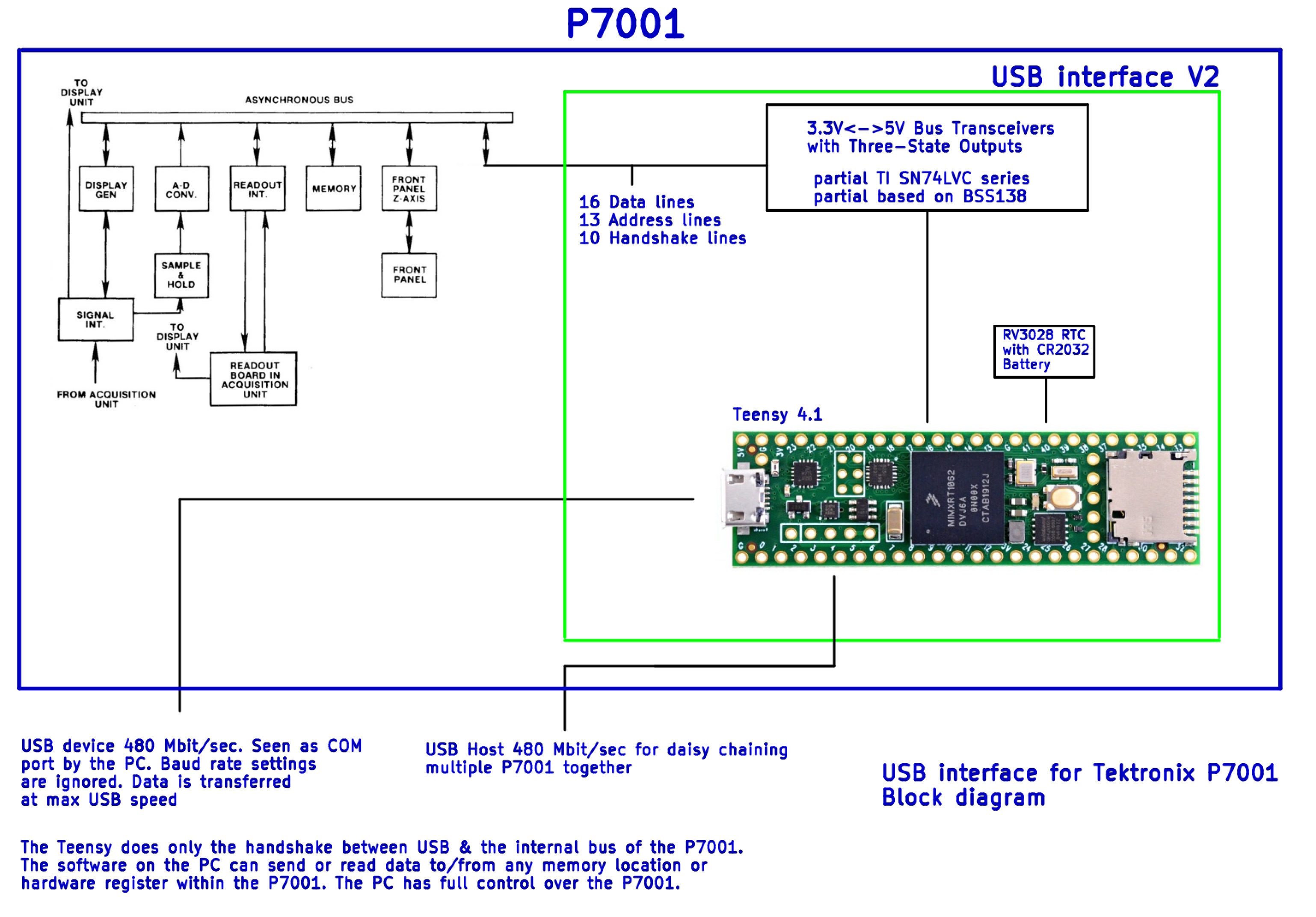
The USB Interface is directly attached to the internal bus of the P7001. This allows not only to directly interact with every other card in the instrument - it also provides the maximum communication speed.
The central component of the board is a Teensy 4.1 USB development board from PJRC. The only other components are level shifters between the 5V environment of the P7001 and the 3.3V environment of the Teensy. The complete handshake is done in software within the Teensy.
The internal bus of the P7001 provides a lot of signals. Beside 16 data and 13 address lines, we have 15 generic handshake lines plus 16 “reserved” handshake lines which are used for direct communication between some of the internal cards. An external interface can use 10 of these handshake lines. This sums up to 39 lines in total. The last two IO pins of the Teensy were used for the communication with the RTC module.
For most of the signals, the TI SN74LVC8T245PW was used as level shifter. This was a bit of a compromise. I would have preferred at least the 16 bit variant of this chip and initially I even wanted to use a completely different vendor. But in order to keep the costs within reasonable bounds, I had to resort to an IC that was in stock at the manufacturer of the PCB. It’s a very good IC which does the job perfectly - I simply didn’t have it in mind when I was thinking about the design.
Taking the BSS138 for the remaining handshake lines was straight forward. The only requirement here was to find one with fast switching times. Choosing a high quality brand like Infineon solved that problem.